


look at the future of chips from Intel's first Chiplet design.
Source: The content is compiled by Semiconductor Industry Watch (ID:icbank) from 「anandtech", thank you.
Sapphire Rapids:

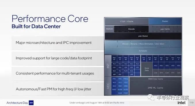
Golden Cove: High-performance kernel with AMX and AIA
-
16B → 32B length decode -
4-wide → 6-wide decode -
5K → 12K branch targets -
2.25K → 4K μop cache -
5 → 6 wide allocation -
10 → 12 execution ports -
352 → 512-entry reorder buffer


an adverb about CXL

Forward to More Silicon: Connectivity Is Important


Sapphire Rapids
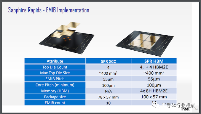
All about Tiles

-
Core, Cache, and Grid -
Memory Controller with 2x 64-bit DDR5 Channel -
UPI link -
accelerator link -
PCIe link
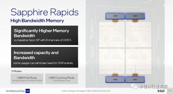
Add some HBM and Optane

UPI link

security
conclusion
Created on:2021年8月31日 15:11